
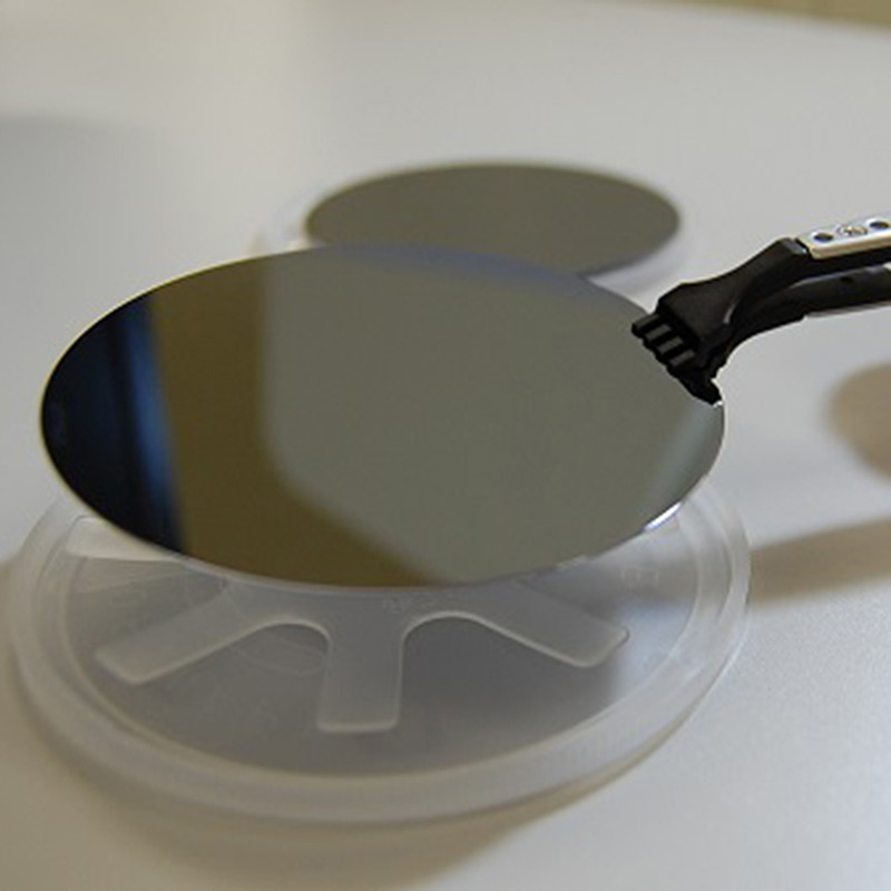


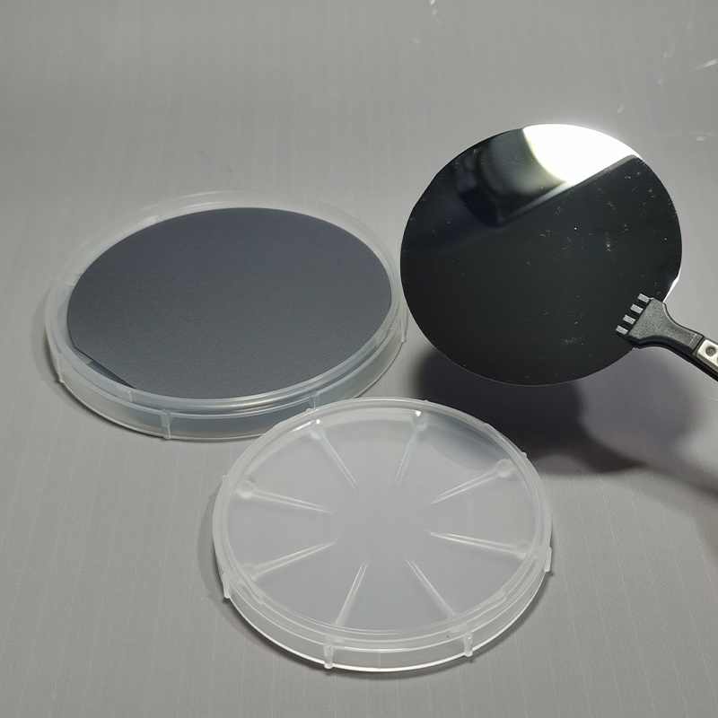
| No. | Items | Standard Specification | |||
| 1 | Size | 2″ | 3″ | 4″ | 6″ |
| 2 | Diameter mm | 50.8±0.3 | 76.2±0.3 | 100±0.5 | 150±0.5 |
| 3 | Growth Method | VGF | VGF | VGF | VGF |
| 4 | Conductivity Type | P/Zn, N/Si, Semi-insulating | |||
| 5 | Orientation | (100)±0.5° | (100)±0.5° | (100)±0.5° | (100)±0.5° |
| 6 | Thickness μm | 350±25 | 625±25 | 625±25 | 650±25 |
| 7 | Orientation Flat mm | 17±1 | 22±1 | 32±1 | Notch |
| 8 | Identification Flat mm | 7±1 | 12±1 | 18±1 | - |
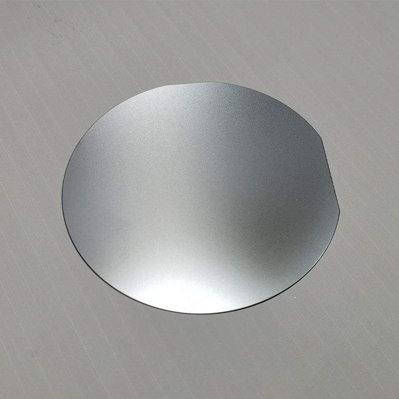
| 9 | Resistivity Ω-cm | (1-9)E(-3) for P or N, (1-10)E8 for semi-insulating | |||
| 10 | Mobility cm2/v.s | 50-120 for P, (1-2.5)E3 for N; ≥4000 for semi-insulating | |||
| 11 | Carrier Concentration cm-3 | (5-50)E18 for P; (0.8-4)E18 for N | |||
| 12 | TTV μm max | 10 | 10 | 10 | 10 |
| 13 | Bow μm max | 30 | 30 | 30 | 30 |
| 14 | Warp μm max | 30 | 30 | 30 | 30 |
| 15 | EPD cm-2 | 5000 | 5000 | 5000 | 5000 |
| 16 | Surface Finish | P/E, P/P | P/E, P/P | P/E, P/P | P/E, P/P |
| 17 | Packing | Single wafer container sealed in Aluminum bag. | |||
| 18 | Mechanical Grade GaAs wafer regardless of electronic specifications also available. | ||||
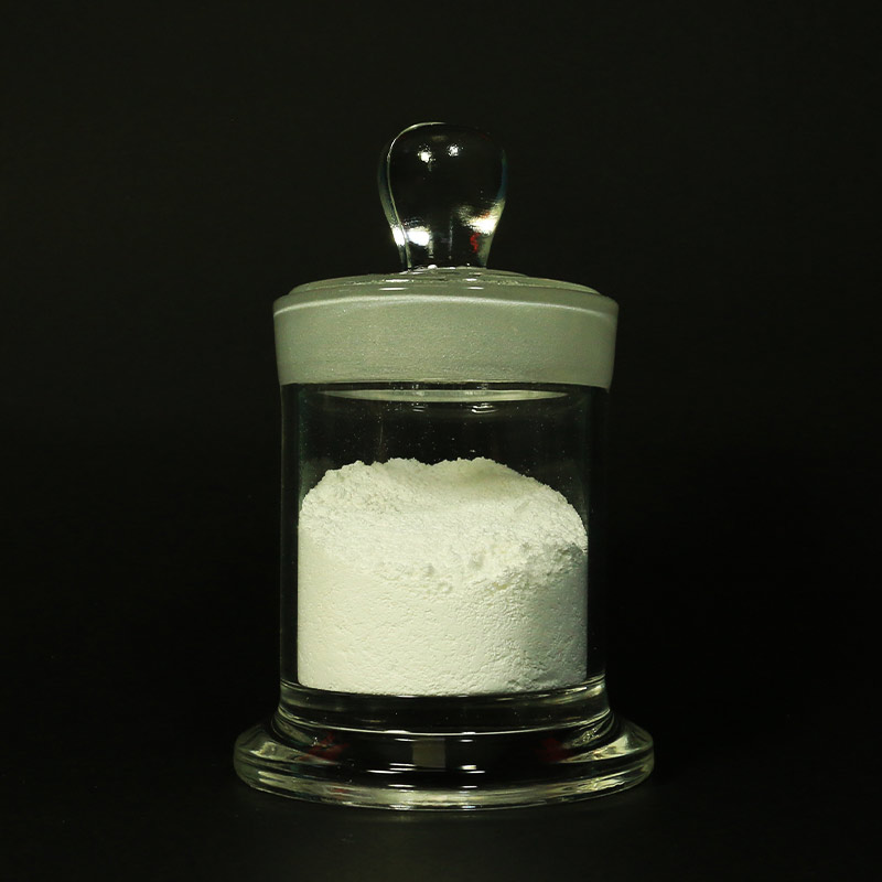
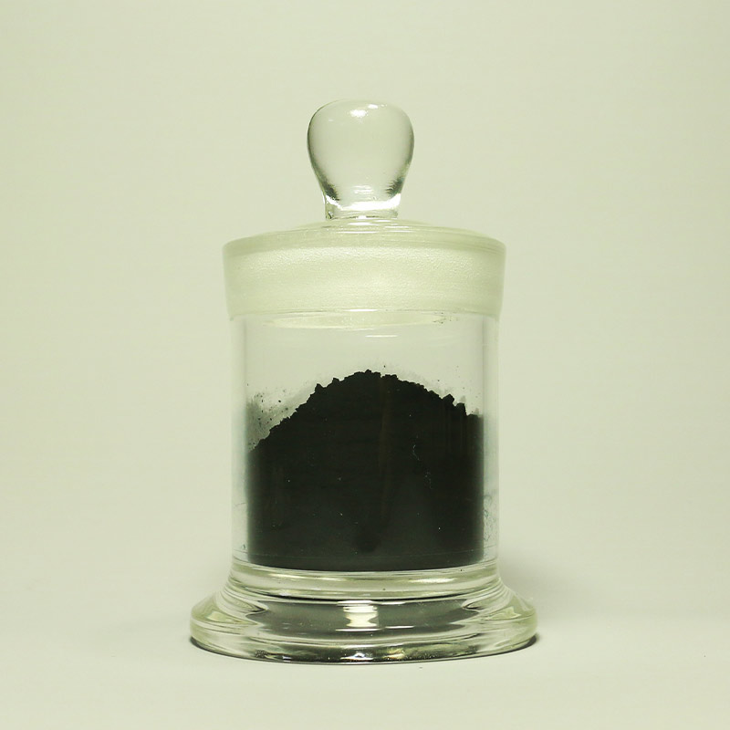
| Linear Formula | GaAs |
| Molecular Weight | 144.64 |
| Crystal structure | Zinc blende |
| Apperance | Gray crystalline solid |
| Melting Point | 1400°C, 2550°F |
| Boiling Point | N/A |
| Density at 300K | 5.32 g/cm3 |
| Energy Gap | 1.424 eV |
| Intrinsic resistivity | 3.3E8 Ω-cm |
| CAS Number | 1303-00-0 |
| EC Number | 215-114-8 |
- Sample Available Upon Request
- Safety Delivery of Goods By Courier/Air/Sea
- COA/COC Quality Management
- Secure & Convenient Packing
- UN Standard Packing Available Upon Request
- Quality Inspection Including XRD/SEM/ICP/GDMS etc
- Full Scope of Trade Terms CPT/FOB/ CFR/CIP By Incoterms 2010
- Flexible Payment Terms T/T D/P L/C Acceptable
- Full Dimensional After-Sale Services
- ISO9001:2015 Certified & Rohs/REACH Regulations Approval
- Non-Disclosure Agreements
- Non-Conflict Mineral Policy
- Regular Environmental Management Review
- Social Responsibility Fulfillment
