- info@matltech.com
- E2-1-1011 Global Center, No.1700 Tianfu Avenue North, Chengdu 610041, China.


Details
Tags
| No. | Items | Standard Specification | ||
| 1 | General Characteristics | |||
| 1-1 | Size | 4″ | 5″ | 6″ |
| 1-2 | Diameter mm | 100±0.5 | 125±0.5 | 150±0.5 |
| 1-3 | Orientation | <100>, <111> | <100>, <111> | <100>, <111> |
| 2 | Epitaxial Layer Characteristics | |||
| 2-1 | Growth Method | CVD | CVD | CVD |
| 2-2 | Conductivity Type | P or P+, N/ or N+ | P or P+, N/ or N+ | P or P+, N/ or N+ |
| 2-3 | Thickness μm | 2.5-120 | 2.5-120 | 2.5-120 |
| 2-4 | Thickness Uniformity | ≤3% | ≤3% | ≤3% |
| 2-5 | Resistivity Ω-cm | 0.1-50 | 0.1-50 | 0.1-50 |
| 2-6 | Resistivity Uniformity | ≤3% | ≤5% | - |
| 2-7 | Dislocation cm-2 | <10 | <10 | <10 |
| 2-8 | Surface Quality | No chip, haze or orange peel remains, etc. | ||
| 3 | Handle Substrate Characteristics | |||
| 3-1 | Growth Method | CZ | CZ | CZ |
| 3-2 | Conductivity Type | P/N | P/N | P/N |
| 3-3 | Thickness μm | 525-675 | 525-675 | 525-675 |
| 3-4 | Thickness Uniformity max | 3% | 3% | 3% |
| 3-5 | Resistivity Ω-cm | As required | As required | As required |
| 3-6 | Resistivity Uniformity | 5% | 5% | 5% |
| 3-7 | TTV μm max | 10 | 10 | 10 |
| 3-8 | Bow μm max | 30 | 30 | 30 |
| 3-9 | Warp μm max | 30 | 30 | 30 |
| 3-10 | EPD cm-2 max | 100 | 100 | 100 |
| 3-11 | Edge Profile | Rounded | Rounded | Rounded |
| 3-12 | Surface Quality | No chip, haze or orange peel remains, etc. | ||
| 3-13 | Back Side Finish | Etched or LTO (5000±500Å) | ||
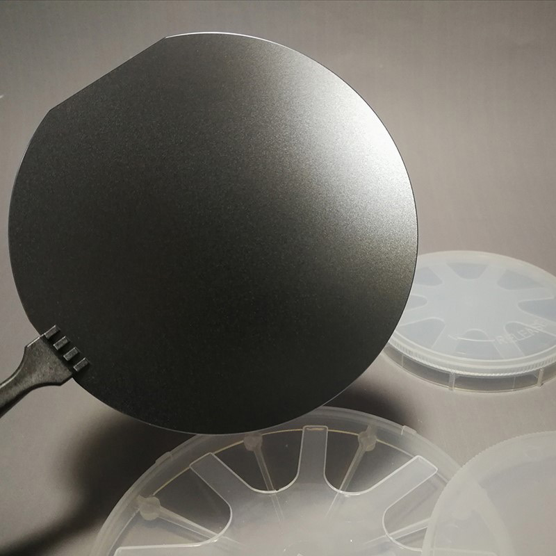
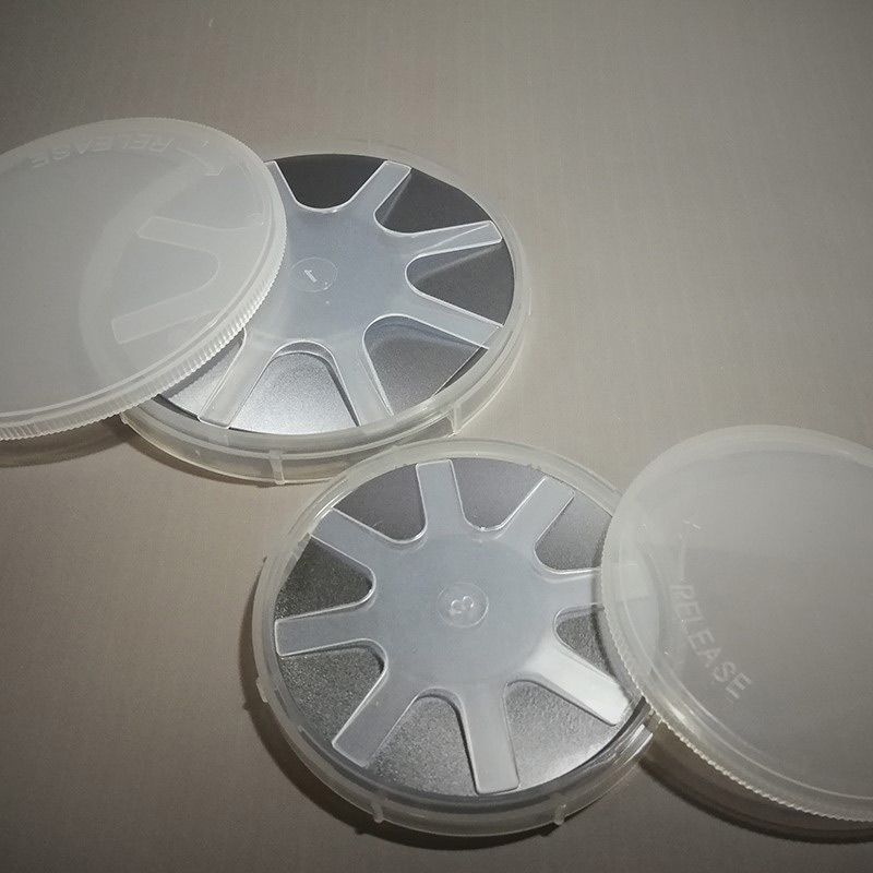
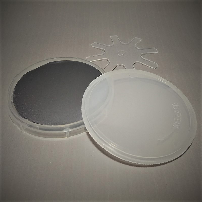
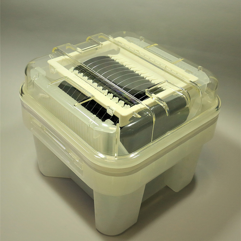
| 4 | Packing | Cassette inside, carton box outside. | ||
- Sample Available Upon Request
- Safety Delivery of Goods By Courier/Air/Sea
- COA/COC Quality Management
- Secure & Convenient Packing
- UN Standard Packing Available Upon Request
- ISO9001:2015 Certified
- CPT/CIP/FOB/CFR Terms By Incoterms 2010
- Flexible Payment Terms T/T D/P L/C Acceptable
- Full Dimensional After-Sale Services
- Quality Inspection By Sate-of-the-art Facility
- Rohs/REACH Regulations Approval
- Non-Disclosure Agreements NDA
- Non-Conflict Mineral Policy
- Regular Environmental Management Review
- Social Responsibility Fulfillment
