- info@matltech.com
- E2-1-1011 Global Center, No.1700 Tianfu Avenue North, Chengdu 610041, China.


Details
Tags
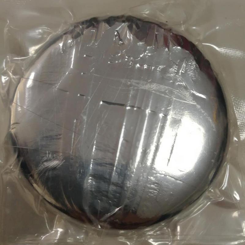
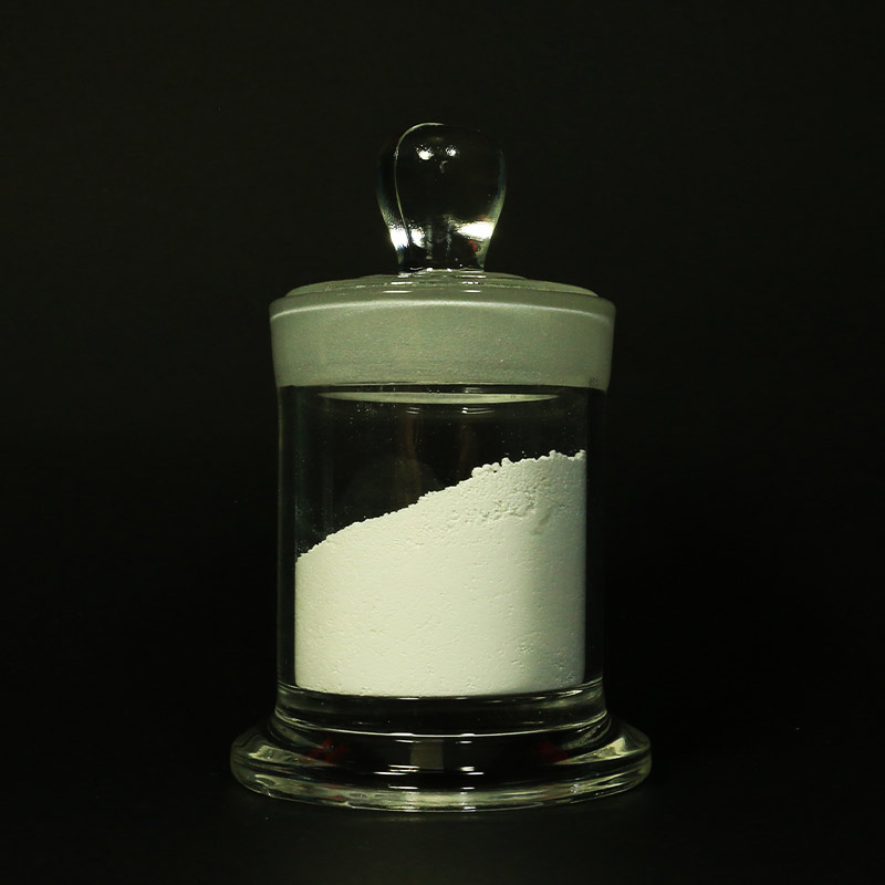
| No. | Items | Standard Specification | |
| 1 | Size | 2″, 3″, 4″, 5″, 6″, 8″, 9.5″, 10″, 12″ | |
| 2 | Diameter mm | 50.8-241.3, or as required | |
| 3 | Growth Method | CZ, MCZ, FZ, FZ-NTD | |
| 4 | Conductivity Type | P-type/B doped, N-type/P-doped or Un-doped | |
| 5 | Length mm | ≥180 or as required | |
| 6 | Orientation | <100>, <110>, <111> | |
| 7 | Resistivity Ω-cm | As required | |
| 8 | Carbon Content a/cm3 | ≤5E16 or as required | |
| 9 | Oxygen Content a/cm3 | ≤1E18 or as required | |
| 10 | Metal Contamination a/cm3 | <5E10 (Cu, Cr, Fe, Ni) or <3E10 (Al, Ca, Na, K, Zn) | |
| 11 | Packing | Plastic bag inside, carton box outside. | |
| Symbol | Si |
| Atomic Number | 14 |
| Atomic Weight | 28.09 |
| Element Category | Metalloid |
| Group, Period, Block | 14, 3, P |
| Crystal structure | Diamond |
| Color | Dark gray |
| Melting Point | 1414°C, 2577.2°F, 1687.15 K |
| Boiling Point | 3265°C, 5909°F, 3538.15 K |
| Density at 300K | 2.329 g/cm3 |
| Intrinsic resistivity | 3.2E5 Ω-cm |
| CAS Number | 7440-21-3 |
| EC Number | 231-130-8 |
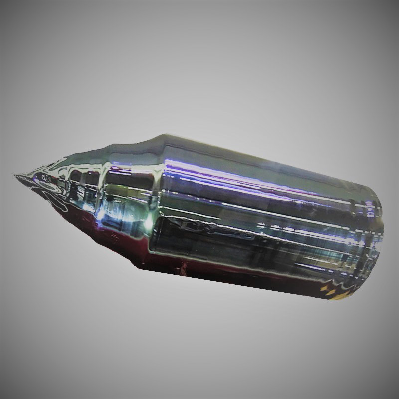
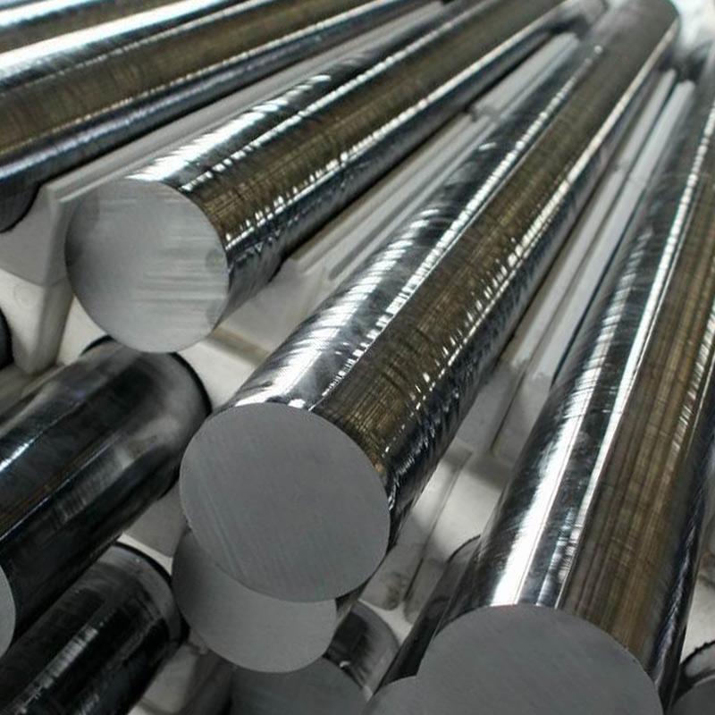
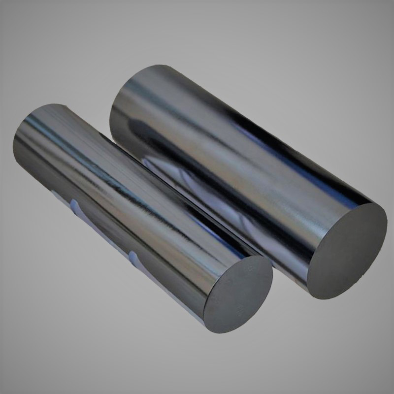
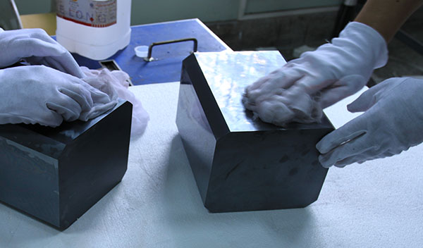
Single Crystal Silicon Ingot, when completely grown and qualified its resistivity, impurity content, crystal perfection, size and weight, is grounded using diamond wheels to make it a perfect cylinder to the right diameter, then undergoes an etching process to remove the mechanical defects left by the grinding process. Afterwards the cylindrical ingot is cut into blocks with certain length, and is given notch and primary or secondary flat by automated wafer handling systems for alignment to identify the crystallographic orientation and conductivity before downstream wafer slicing process.
- Sample Available Upon Request
- Safety Delivery of Goods By Courier/Air/Sea
- COA/COC Quality Management
- Secure & Convenient Packing
- UN Standard Packing Available Upon Request
- ISO9001:2015 Certified
- CPT/CIP/FOB/CFR Terms By Incoterms 2010
- Flexible Payment Terms T/T D/P L/C Acceptable
- Full Dimensional After-Sale Services
- Quality Inspection By Sate-of-the-art Facility
- Rohs/REACH Regulations Approval
- Non-Disclosure Agreements NDA
- Non-Conflict Mineral Policy
- Regular Environmental Management Review
- Social Responsibility Fulfillment

1.jpg)


