- info@matltech.com
- E2-1-1011 Global Center, No.1700 Tianfu Avenue North, Chengdu 610041, China.


FZ Silicon Wafer
Description
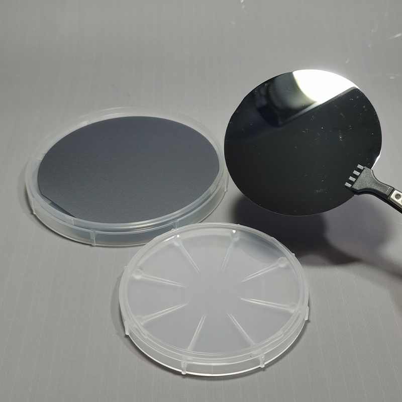
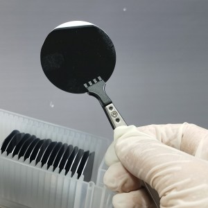
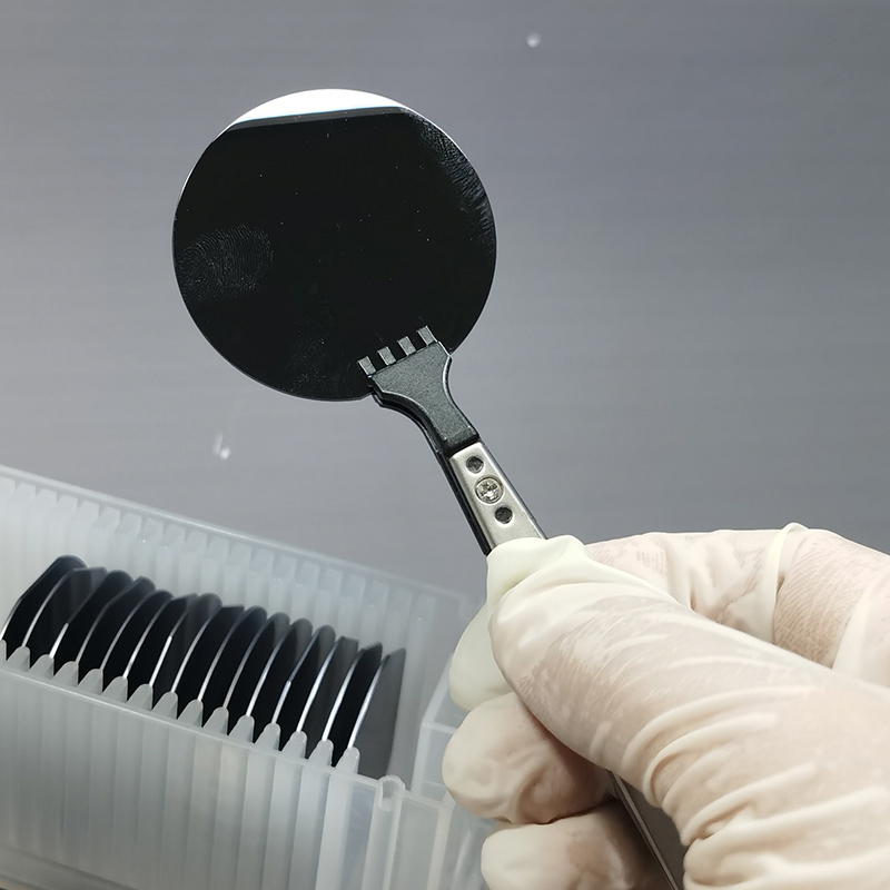
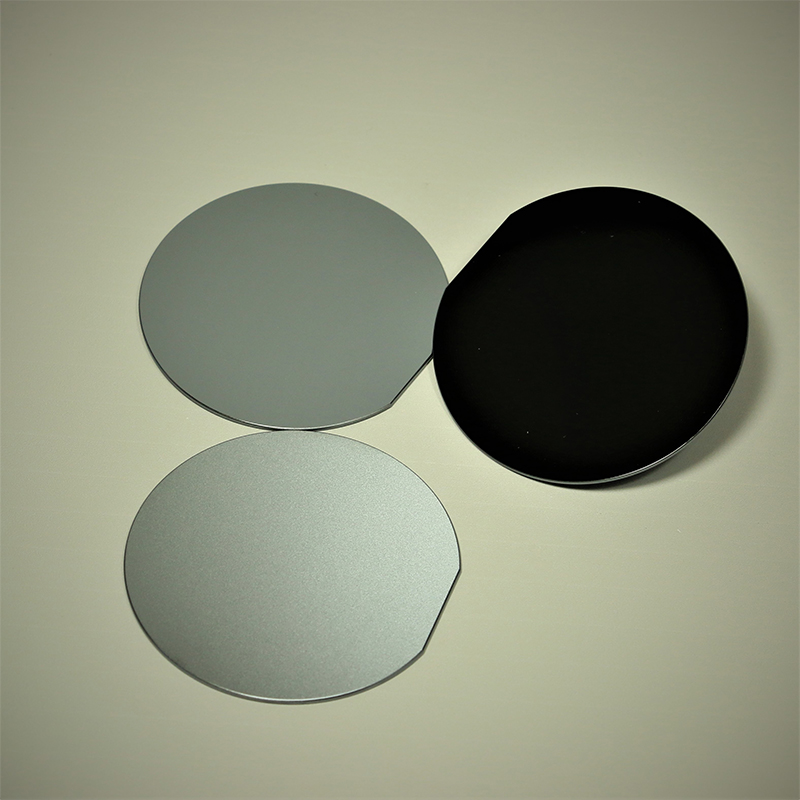
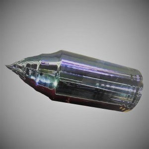
FZ Single Crystal Silicon Wafer, Float-zone (FZ) Silicon is extremely pure silicon with a very low concentration of oxygen and carbon impurities pulled by vertical floating zone refining technology. FZ Floating zone is a single crystal ingot growing method which is different from CZ method wherein seed crystal is attached under polycrystalline silicon ingot, and border between seed crystal and polycrystalline crystal silicon is melted by RF coil induction heating for single crystallization. The RF coil and the melted zone move upwards, and a single crystal solidifies on top of the seed crystal accordingly. Float-zone silicon is ensured with a uniform dopant distribution, lower resistivity variation, restrict amounts of impurities, considerable carrier lifetime, high resistivity target and high purity silicon. Float-zone silicon is a high-purity alternative to crystals grown by the Czochralski CZ process. With the characteristics of this method, FZ Single Crystal Silicon is ideal for use in electronic devices fabrication, such as diodes, thyristors, IGBTs, MEMS, diode, RF device and power MOSFETs, or as the substrate for high-resolution particle or optical detectors, power devices and sensors, high efficiency solar cell etc.
Delivery
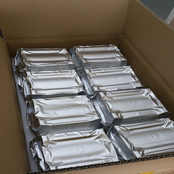
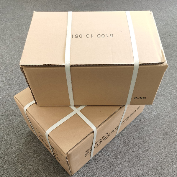
FZ Single Crystal Silicon Wafer N-type and P-type conductivity at Western Minmetals (SC) Corporation can be delivered in size of 2, 3, 4, 6 and 8 inch (50mm, 75mm, 100mm, 125mm, 150mm and 200mm) and orientation <100>, <110>, <111> with surface finish of As-cut, Lapped, etched and polished in package of foam box or cassette with carton box outside.
Details
Tags
Technical Specification
FZ Single Crystal Silicon Wafer or FZ Mono-crystal Silicon Wafer of intrinsic, n-type and p-type conductivity at Western Minmetals (SC) Corporation can be delivered in various size of 2, 3, 4, 6 and 8 inch in diameter (50mm, 75mm, 100mm, 125mm, 150mm and 200mm) and wide range of thickness from 279um up to 2000um in <100>, <110>, <111> orientation with surface finish of as-cut, lapped, etched and polished in package of foam box or cassette with carton box outside.
| No. | Items | Standard Specification | ||||
| 1 | Size | 2" | 3" | 4" | 5" | 6" |
| 2 | Diameter mm | 50.8±0.3 | 76.2±0.3 | 100±0.5 | 125±0.5 | 150±0.5 |
| 3 | Conductivity | N/P | N/P | N/P | N/P | N/P |
| 4 | Orientation | <100>, <110>, <111> | ||||
| 5 | Thickness μm | 279, 381, 425, 525, 575, 625, 675, 725 or as required | ||||
| 6 | Resistivity Ω-cm | 1-3, 3-5, 40-60, 800-1000, 1000-1400 or as required | ||||
| 7 | RRV max | 8%, 10%, 12% | ||||
| 8 | TTV μm max | 10 | 10 | 10 | 10 | 10 |
| 9 | Bow/Warp μm max | 30 | 30 | 30 | 30 | 30 |
| 10 | Surface Finish | As-cut, L/L, P/E, P/P | ||||
| 11 | Packing | Foam box or cassette inside, carton box outside. | ||||
| Symbol | Si |
| Atomic Number | 14 |
| Atomic Weight | 28.09 |
| Element Category | Metalloid |
| Group, Period, Block | 14, 3, P |
| Crystal structure | Diamond |
| Color | Dark gray |
| Melting Point | 1414°C, 1687.15 K |
| Boiling Point | 3265°C, 3538.15 K |
| Density at 300K | 2.329 g/cm3 |
| Intrinsic resistivity | 3.2E5 Ω-cm |
| CAS Number | 7440-21-3 |
| EC Number | 231-130-8 |
FZ Single Crystal Silicon, with the paramount characteristics of Float-zone (FZ) method, is an ideal for use in electronic devices fabrication, such as diodes, thyristors, IGBTs, MEMS, diode, RF device and power MOSFETs, or as the substrate for high-resolution particle or optical detectors, power devices and sensors, high efficiency solar cell etc.
Procurement Tips
- Sample Available Upon Request
- Safety Delivery of Goods By Courier/Air/Sea
- COA/COC Quality Management
- Secure & Convenient Packing
- UN Standard Packing Available Upon Request
- ISO9001:2015 Certified
- CPT/CIP/FOB/CFR Terms By Incoterms 2010
- Flexible Payment Terms T/T D/P L/C Acceptable
- Full Dimensional After-Sale Services
- Quality Inspection By Sate-of-the-art Facility
- Rohs/REACH Regulations Approval
- Non-Disclosure Agreements NDA
- Non-Conflict Mineral Policy
- Regular Environmental Management Review
- Social Responsibility Fulfillment
FZ Silicon Wafer
- English
- French
- German
- Portuguese
- Spanish
- Russian
- Japanese
- Korean
- Arabic
- Irish
- Greek
- Turkish
- Italian
- Danish
- Romanian
- Indonesian
- Czech
- Afrikaans
- Swedish
- Polish
- Basque
- Catalan
- Esperanto
- Hindi
- Lao
- Albanian
- Amharic
- Armenian
- Azerbaijani
- Belarusian
- Bengali
- Bosnian
- Bulgarian
- Cebuano
- Chichewa
- Corsican
- Croatian
- Dutch
- Estonian
- Filipino
- Finnish
- Frisian
- Galician
- Georgian
- Gujarati
- Haitian
- Hausa
- Hawaiian
- Hebrew
- Hmong
- Hungarian
- Icelandic
- Igbo
- Javanese
- Kannada
- Kazakh
- Khmer
- Kurdish
- Kyrgyz
- Latin
- Latvian
- Lithuanian
- Luxembou..
- Macedonian
- Malagasy
- Malay
- Malayalam
- Maltese
- Maori
- Marathi
- Mongolian
- Burmese
- Nepali
- Norwegian
- Pashto
- Persian
- Punjabi
- Serbian
- Sesotho
- Sinhala
- Slovak
- Slovenian
- Somali
- Samoan
- Scots Gaelic
- Shona
- Sindhi
- Sundanese
- Swahili
- Tajik
- Tamil
- Telugu
- Thai
- Ukrainian
- Urdu
- Uzbek
- Vietnamese
- Welsh
- Xhosa
- Yiddish
- Yoruba
- Zulu
