- info@matltech.com
- E2-1-1011 Global Center, No.1700 Tianfu Avenue North, Chengdu 610041, China.


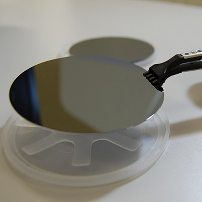
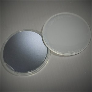
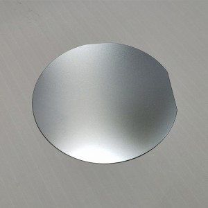
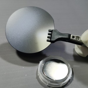
High Quality Fzntd - Gallium Arsenide GaAs – WMC
Cadmium Telluride CdTe, cubic zincblende crystal, is II-VI crystalline compound semiconductor synthesized from cadmium and tellurium with purity of 99.999%, 99.9999% and 99.99999% (5N 6N 7N), it can be crystallized from the Te-rich Cd-Te solution by Traveling Heater Method (THM).
Being high resistivity at room temperature and large linear attenuation coefficient, CdTe became to be considered a prospective material for the room temperature semiconductor detector, it is primarily employed for several applications such as an infrared optical window and lens, thin film solar cell material, PIN semiconductor structure manufacturing, Infrared imaging, X-ray and gamma ray detection, optical devices, and photovotaic, epitaxial substrate; evaporation source of crystal sheet, electro-optic modulators designing or target materials epitaxial processing and other related fields. Besides, CdTe crystals can be used for spectral analysis and far infrared transmission and can be alloyed with mercury to make a versatile HgCdTe MCT infrared detector material, and alloyed with zinc to make CdZnTe solid x-ray and gamma ray detector.
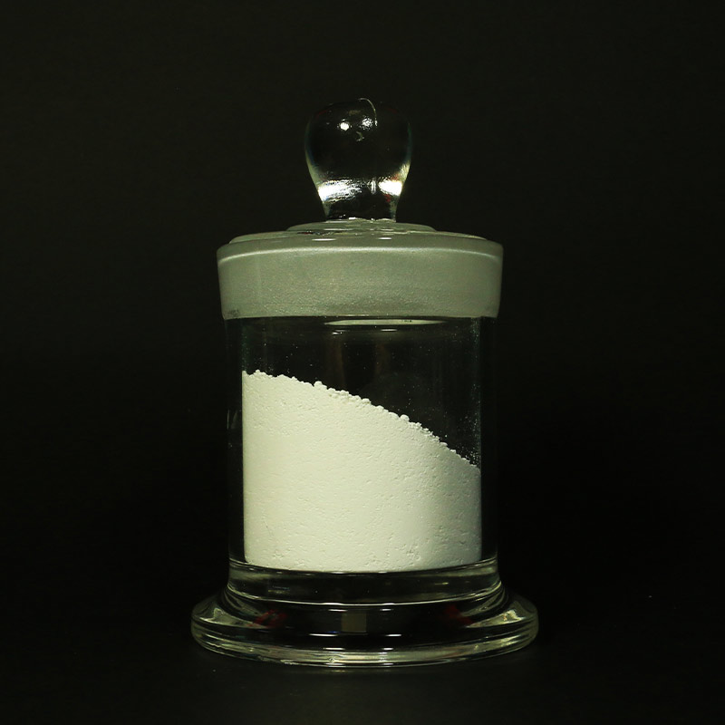
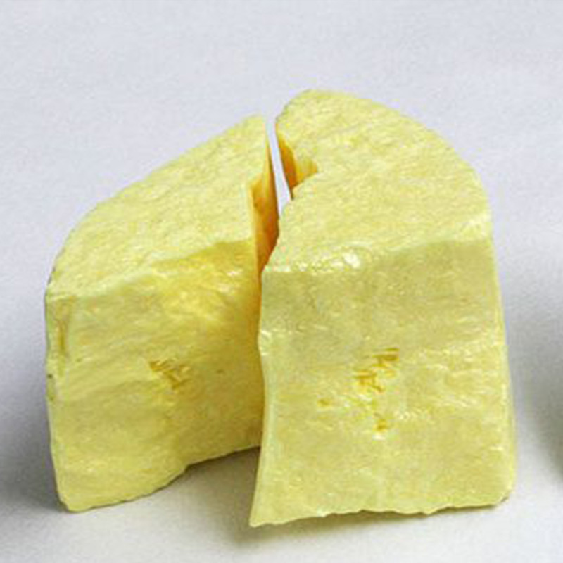
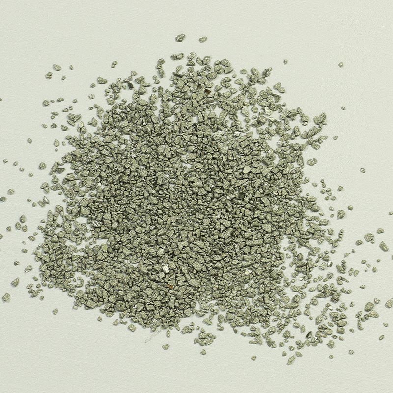
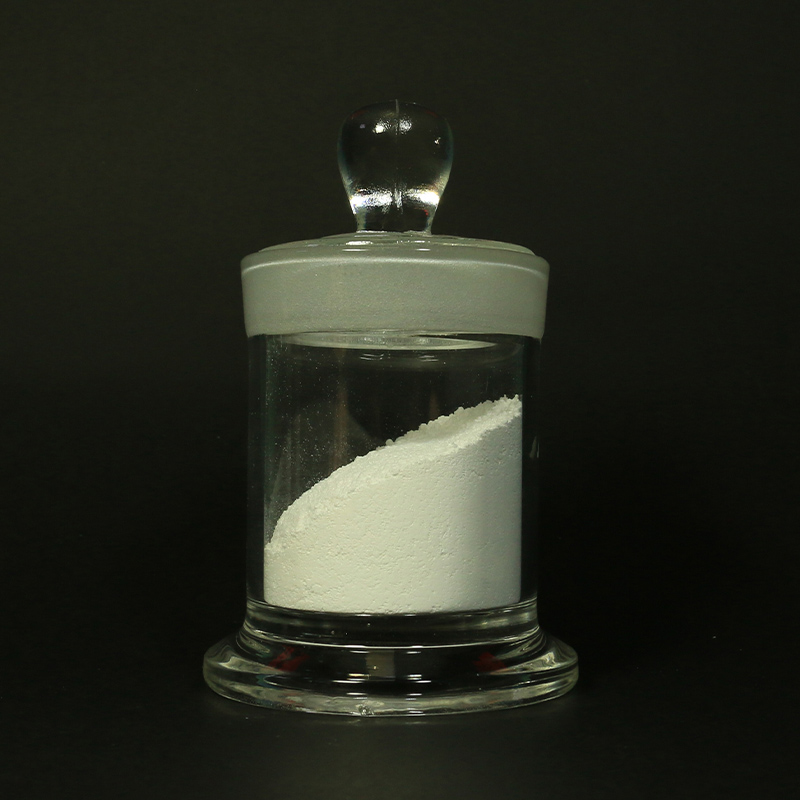
Cadmium Telluride CdTe polycrystalline at Western Minmetals (SC) Corporation with 99.999% 99.9999%, 99.99999% 5N 6N 7N purity is in size of powder, lump, chunk, and bar or customized specification can be delivered, which is packed in composite aluminum bag with argon gas filled protection, carton box outside, and Cadmium Telluride CdTe single crystal at Western Minmetals (SC) Corporation delivered with 99.999% 99.9999%, 99.99999% 5N 6N 7N purity is in form of bar and blank 5x5x0.5mm, 10x10x0.5m, and Disc with 1.0 inch in diameter x 0.5mm or customized specification.
.
Details
Tags
| No. | Items | Standard Specification | |||
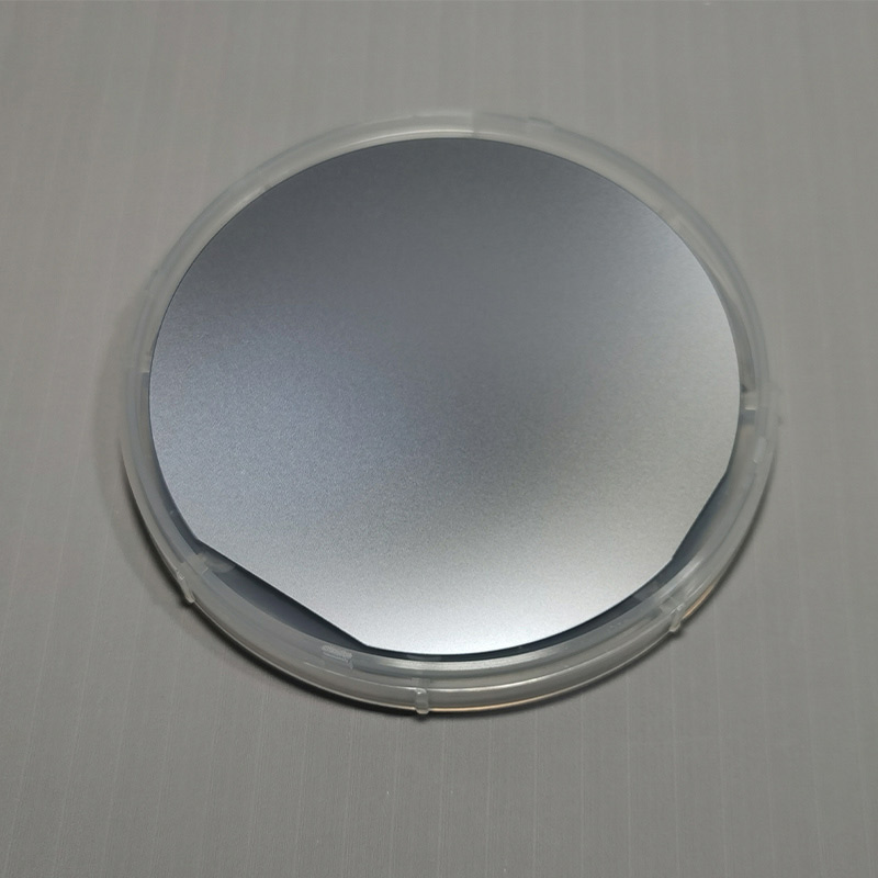
| 1 | Size | 2″ | 3″ | 4″ | 6″ |
| 2 | Diameter mm | 50.8±0.3 | 76.2±0.3 | 100±0.5 | 150±0.5 |
| 3 | Growth Method | VGF | VGF | VGF | VGF |
| 4 | Conductivity Type | P/Zn, N/Si, Semi-insulating | |||
| 5 | Orientation | (100)±0.5° | (100)±0.5° | (100)±0.5° | (100)±0.5° |
| 6 | Thickness μm | 350±25 | 625±25 | 625±25 | 650±25 |
| 7 | Orientation Flat mm | 17±1 | 22±1 | 32±1 | Notch |
| 8 | Identification Flat mm | 7±1 | 12±1 | 18±1 | - |
| 9 | Resistivity Ω-cm | (1-9)E(-3) for P or N, (1-10)E8 for semi-insulating | |||
| 10 | Mobility cm2/v.s | 50-120 for P, (1-2.5)E3 for N; ≥4000 for semi-insulating | |||
| 11 | Carrier Concentration cm-3 | (5-50)E18 for P; (0.8-4)E18 for N | |||
| 12 | TTV μm max | 10 | 10 | 10 | 10 |
| 13 | Bow μm max | 30 | 30 | 30 | 30 |
| 14 | Warp μm max | 30 | 30 | 30 | 30 |
| 15 | EPD cm-2 | 5000 | 5000 | 5000 | 5000 |
| 16 | Surface Finish | P/E, P/P | P/E, P/P | P/E, P/P | P/E, P/P |
| 17 | Packing | Single wafer container sealed in Aluminum bag. | |||
| 18 | Mechanical Grade GaAs wafer regardless of electronic specifications also available. | ||||
| Linear Formula | GaAs |
| Molecular Weight | 144.64 |
| Crystal structure | Zinc blende |
| Apperance | Gray crystalline solid |
| Melting Point | 1400°C, 2550°F |
| Boiling Point | N/A |
| Density at 300K | 5.32 g/cm3 |
| Energy Gap | 1.424 eV |
| Intrinsic resistivity | 3.3E8 Ω-cm |
| CAS Number | 1303-00-0 |
| EC Number | 215-114-8 |
- Sample Available Upon Request
- Safety Delivery of Goods By Courier/Air/Sea
- COA/COC Quality Management
- Secure & Convenient Packing
- UN Standard Packing Available Upon Request
- Quality Inspection Including XRD/SEM/ICP/GDMS etc
- Full Scope of Trade Terms CPT/FOB/ CFR/CIP By Incoterms 2010
- Flexible Payment Terms T/T D/P L/C Acceptable
- Full Dimensional After-Sale Services
- ISO9001:2015 Certified & Rohs/REACH Regulations Approval
- Non-Disclosure Agreements
- Non-Conflict Mineral Policy
- Regular Environmental Management Review
- Social Responsibility Fulfillment
